The world and our interaction with it is analog. Our surrounding environment, colors in the electromagnetic spectrum, speech, and sound all are represented by continuously changing analog values. When it comes to processing these analog signals, however, digital systems offer several benefits to a traditional analog processing solution. For example, they have higher performance, ease of storage and transmission, and better noise immunity. As such, while the world is analog, it is mainly processed digitally using logic circuits. In this learning module, you will be introduced to the essentials of logic design, and how it can be implemented using programmable logic.
2. Objectives
Upon completion of this module, you will be able to:
 Perform some fundamental operations of Boolean algebra
 Explain the operation and truth tables of common logic gates
 Illustrate how combinatorial circuits are designed
 Discuss the differences between combinatorial and sequential circuits
 Understand how shift registers, counters, and state machines operate
 Explain the basic structures of PLDs
The key foundation of digital logic is Boolean Algebra. Without understanding it we cannot produce effective logic designs or understand the outputs of higher level tools such as synthesis engines.
Boolean algebra is named after its inventor, George Boole, who in 1854 published his work entitled, "An investigation of the laws of thought on which are founded the mathematical theories of logic and probabilities." This work was later used by Claude Shannon in his 1937 master's thesis at MIT entitled, "A Symbolic Analysis of Relay and Switching Circuits," which demonstrated that switching circuits could solve all problems in the same manner as Boolean algebra. Thus, the relationship between switching circuits and Boolean algebra became the foundation of all digital applications.
- 3.1 Boolean Addition and Multiplication
0+0=0 1+0=1 0+1=1 1+1=1
As you can see, the result of the SUM is equal to one only when one or more of the literals is one.
Boolean multiplication produces the PRODUCT of the literals:
0.0=0 1.0=0 0.1=0 1.1=1
In this case, you can see the PRODUCT is equal to one only when both literals are equal to one.
Understanding the meaning of the SUM and PRODUCT terms will be important later when we examine logic gates and equations.
- 3.2 Boolean Algebra Laws
Just as in other areas of mathematics, Boolean algebra has several laws which we must understand, such as:
 Commutative Law: The order of literals in Boolean addition does not affect the result: A+B=B+A
 Associative Law: When performing Boolean addition of more than two literals, the result is the same regardless of grouping: A+(B+C)=(A+B)+C
 Distributive Law: Performing a Boolean addition of two or more literals before performing a Boolean multiplication on the result is the same as performing the Boolean multiplication with each literal before performing the Boolean Addition A(B+C)=AB+AC
These laws become very important when we design logic circuits and wish to optimize the number of logic gates we use in our solution.
Along with these laws we also have twelve rules of Boolean Logic with which we must become familiar. They are:
| 12 Boolean Logic Rules | |
|---|---|
| A + 0 = A | A . A = A |
| A + 1 = 1 | A . A = 0 |
| A . 0 = 0 |  = A = A |
| A . 1 = A | A + A.B = A |
| A + A = A | A + A.B = A + B |
| A + A = 1 | (A + B).(A+C) = A + B.C |
- 3.3 DeMorgan's Theorem
The final remaining element we need to understand about Boolean Algebra is DeMorgan's Theorem which states, "The complement of a product of sums is equal to the sum of the complements."
This is better shown represented as an equation: A.B = A + B
A good mnemonic device to remember this is: "break the bar, change the sign."
Of course, now that we understand Boolean algebra, we want to be able to see how it maps to the logic gates we use to implement digital circuits.
The seven commonly used logic gates in digital design are NOT, AND, OR, XOR, NOR, NAND and XNOR gates. In our designs we use combinations of these logic gates to implement the logic function. In this section, we'll review these logic gates.
At the lowest level these logic gates are made from arrangements of transistors; however, each arrangement has its own symbol and truth table, which shows for a given input what its outputs will be. (Note: For simplicity's sake, except for the NOT gate, all gates are demonstrated with two inputs).
- 4.1 NOT Gate
The simplest of the logic gates is the NOT gate. This gate simply inverts the logic value presented on the input.
NOT symbol & truth table
| Input | Output |
|---|---|
| 0 | 1 |
| 1 | 0 |
Figure 1: NOT Gate
- 4.2 AND Gate
One of the most commonly used logic gates is the AND gate, which implements Boolean algebra multiplication and produces the PRODUCT of its inputs as we described earlier in this learning module.
AND Symbol & Truth Table
| Input A | Input B | Output |
|---|---|---|
| 0 | 0 | 0 |
| 0 | 1 | 0 |
| 1 | 0 | 0 |
| 1 | 1 | 1 |
Figure 2: AND Gate
- 4.3 OR Gate
To implement Boolean addition and generate the SUM of its inputs, we use the OR Gate which uses the symbol as shown in Figure 3.
OR Symbol & Truth Table
| Input A | Input B | Output |
|---|---|---|
| 0 | 0 | 0 |
| 0 | 1 | 1 |
| 1 | 0 | 1 |
| 1 | 1 | 1 |
Figure 3: OR Gate
The remaining logic gates are derivatives of the AND, OR, and NOT functions. However, the NAND and NOR gates have proven to be very popular due to their universality, which allows any logic gate—AND, OR, NOT—to be implemented using these two gates. We will look at exactly how we can do this in an example further on in this learning module.
- 4.4 NAND Gate
The simplest of the gates is the NAND gate, which stands for Not AND. This can be represented by an AND gate followed by a NOT gate. However, it is normally shown as an AND gate with an inversion bubble on its output.
NAND Symbol & Truth Table
| Input A | Input B | Output |
|---|---|---|
| 0 | 0 | 1 |
| 0 | 1 | 1 |
| 1 | 0 | 1 |
| 1 | 1 | 0 |
Figure 4: NAND Gate
- 4.5 NOR Gate
A similar logic gate is the NOR gate, which is also a universal gate and represents the NOT OR function. We represent the NOR symbol as the OR gate with an inversion bubble.
NOR Symbol and Truth Table
| Input A | Input B | Output |
|---|---|---|
| 0 | 0 | 1 |
| 0 | 1 | 0 |
| 1 | 0 | 0 |
| 1 | 1 | 0 |
Figure 5: NOR Gate
- 4.6 XOR and XNOR Gates
The final two gates are the XOR and XNOR gates, which are constructed from logic gates already introduced. However, they provide very useful functions allowing us to determine if both inputs agree (XNOR) or both inputs differ (XOR).
XOR Symbol & Truth Table
| Input A | Input B | Output |
|---|---|---|
| 0 | 0 | 0 |
| 0 | 1 | 1 |
| 1 | 0 | 1 |
| 1 | 1 | 0 |
Figure 6a: XOR Gate
XNOR Symbol & Truth Table
| Input A | Input B | Output |
|---|---|---|
| 0 | 0 | 1 |
| 0 | 1 | 0 |
| 1 | 0 | 0 |
| 1 | 1 | 1 |
Figure 6b: XNOR Gate
As mentioned earlier in this learning module, each of the logic gates consists of several transistors arranged to implement the desired logic gate.
The simplest of these is the NOT gate, which uses two complementary transistors to invert the input at its output. When the Input is high, transistor Q1 is turned off thanks to the inversion, while transistor Q2 is turned on pulling the output to ground, which is the opposite of the presented signal. Conversely, when the input is low, transistor Q2 is this time turned off, while Q1 is turned on, pulling the output to the power rail and outputting a logic high.
This NOT structure is also used in more complex gates such as the AND gate. Looking at the transistor level of the AND gate you will first notice the Output stage Q5 and Q6 is the same as for the NOT gate function.
When inputs A and B are both high, transistors Q1 and Q2 are turned on while Q3 and Q4 are turned off. This pulls the input to Q6 and Q5 low, which due to the inversion means Q5 turns on and Q6 turns off allowing the output to be set high. For all other combinations at least one of Q1, Q2, Q3 and Q4 is turned off ,which pulls the input to Q5 and Q6 high, as such turning on Q6 and off Q5 pulling the output low as would be expected for an AND logic gate.
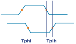
When we implement logic circuits, using logic gates, we call these combinatorial logic circuits as there is no storage or feedback. To ensure these circuits function as intended we also, need to understand what occurs when an input changes. As just demonstrated, logic gates are made up from arrangements of switching transistors, and as such it takes time for a change at an input to result in a change of the output. We call this delay the PROPAGATION time and it will vary depending upon the logic family used.
To ensure we are all on the same page, there are several different logic families, each implemented in different underlying technologies such as CMOS (Complementary Metal Oxide Semi-conductor) or TTL (Transistor to Transistor Logic). Each logic family will exhibit a different propagation delay, which will limit the switching frequency of the logic design. If we are testing in the lab, we measure the propagation delay between the mid-point (50%) of the rising and falling edges as shown below.
Figure 9: Timing Diagram of NOT gate
The propagation time is normally defined within the data sheet for the logic gate selected; however, it will often list two propagation times: one for the high to low transition and another for the low to high transition. Of course, the propagation time will also be affected by the ambient temperature, changes in power supply conditions, resistance of the driver, and the capacitive load on the device output.
We call the output driving several devices inputs the FANOUT. The higher the fanout, the larger the loading, and, therefore, the slower the output rise and fall times. Typical values of propagation time in logic datasheets range from 5 ns to 35 ns, depending upon the logic family, minimum/maximum behavior, and loading conditions (FANOUT).
When we develop our combinatorial circuit, which will typically consist of several levels of logic gates, due to the layer on gates, we need to be careful of the differing propagation delays, as differing propagation delays can lead to glitches in the output value which are not correct. This is one of the reasons that in many applications, combinatorial circuits are used with storage elements like D type flip flops and an associated clock to ensure the output does not glitch and is stable when it is presented to the next processing/decision element.
However, if we are working purely with combinatorial circuits, we can also take some steps to mitigate these glitches, which are often referred to as RACE Hazards.
The best way to demonstrate how we can pull together what we have learned so far about Boolean Algebra, Logic Gates, Propagation Delays, and Hazards is to outline a few simple examples.
For the first example, we will create a system which monitors three motors. Each motor has a health indication output which is high when the motor has a fault. For the overall system to function correctly, at least two of the motors must be working correctly, therefore, we will create a system that outputs a logic high when two out of the three motors have asserted their fault outputs.
The first stage in developing this solution is to create a truth table that shows the possible input combinations and the correct output for each of those input conditions. As we have 3 inputs, then there are 23 or eight possible combinations of the input:
| Input A | Input B | Input C | OP |
|---|---|---|---|
| 0 | 0 | 0 | 0 |
| 0 | 0 | 1 | 0 |
| 0 | 1 | 0 | 0 |
| 0 | 1 | 1 | 1 |
| 1 | 0 | 0 | 0 |
| 1 | 0 | 1 | 1 |
| 1 | 1 | 0 | 1 |
| 1 | 1 | 1 | 1 |
Figure 10: Truth Table for the motor monitoring system's logic function
From this truth table we can generate the following logic equations: OP = (A.B) + (A.C) + (B.C)
We call the format of this equation a SUM of PRODUCTS (SOP) equation as the OP is the Boolean SUM (Logical OR) of the Boolean PRODUCTS (AND) equations.
If we so desired, we could calculate a PRODUCT of SUMS (POS) output by following the approach.
Firstly, we create the SOP logic equation for each entry on the truth table where the output is low: OP = A.B + A.C + B.C

We can then apply DeMorgan's theorem and the ninth law of logic to create the final POS equation: OP=(A+B).(A+C).(B+C)
For the remainder of this example, however, we will work with the SOP format as that is the most common method for implementing logic functions. As such, we can realize our SOP equation using a two-level logic circuit as below:
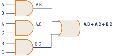
Figure 11: Example Logic Circuit in SOP form
With this two-level network, we need to consider the propagation delay through the first AND gate level and the impact it might have on the output.
Of course, this implementation uses two logic gate types (AND, OR). But it is possible to implement the same logical function using only NAND gates, as they are universal. Thanks to DeMorgan's Theorem, the NAND gate also implements the Negative OR function: A.B = A + B
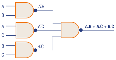
Figure 12: Example Logic Circuit in SOP form implemented using NAND Gates
As such, we can redraw the logic circuit above.
Let's look at how we get the same functionality using NAND gates. The output equation can be represented as: 
Using DeMorgan's Theorem, we can iterate through the following steps, changing the sign as we break the bar and applying other rules of Boolean algebra:

If we are working with POS logic equations, we can use NOR gates to implement the logic equation and prove the functionality the same way using DeMorgan's Theorem and Boolean Algebra rules.
In the example above, we used a truth table to determine the logic equations and it works well for a simple application. However, if we have more complex applications we need a better way of determining the logic equations. This is where the Karnaugh-map (Kmap) comes into play. Kmaps are visual representations of the logic behavior which allow us to use our natural ability for pattern recognition to determine the logic equations.
 |
00 | 01 | 11 | 10 |
|---|---|---|---|---|
| 00 | ||||
| 01 | ||||
| 11 | ||||
| 10 |
Figure 13: Example Karnaugh-map used for four variables (A,B,C,D). Note the gray scale count.
Karnaugh-maps are used by grouping together adjacent 1's for SOP and adjacent 0's for POS. These groupings can then be used to determine the logic equation, using the rules of Boolean Algebra to implement the desired functionality.
 |
00 | 01 | 11 | 10 |
|---|---|---|---|---|
| 00 | 0 | 0 | 0 | 0 |
| 01 | 0 | 1 | 1 | 0 |
| 11 | 0 | 1 | 1 | 0 |
| 10 | 1 | 0 | 0 | 1 |
Figure 14: Example of a Karnaugh-map: Grouping the 1s together.
Often, if we use a Karnaugh-map, we will obtain an equation which uses the minimum number of logic gates to implement. Using the example to the left we can group together the 1's within the design where they are adjacent to each other.
The example groups together four 1's within the center of the Karnaugh-map (highlighted green), and from this we can see that the logic equation is D.B as the C and A cancel each other out due to being across not C and C or not A and A, respectively.
The blue elements in the corner can also be grouped together as they are also judged to be adjacent, since the Karnaugh-map is judged to wrap around edge to edge and top to bottom. As such, the second equation to be extracted from the Karnaugh-map is C.D.B; therefore, the resulting logic equation for the Karnaugh-map is: OP = C.D.B + D.B
We can also use Karnaugh-maps to identify hazards which might result in glitches during operation and help us eliminate them. In the next example, we can extract the logical equation for the green and blue cells as: OP = A.C.D + B.C.D
 |
00 | 01 | 11 | 10 |
|---|---|---|---|---|
| 00 | 0 | 0 | 0 | 0 |
| 01 | 0 | 0 | 0 | 0 |
| 11 | 0 | 1 | 1 | 0 |
| 10 | 1 | 1 | 0 | 0 |
Figure 15: Karnaugh-maps: Identifying Potential Hazards
However, this leaves the equation highlighted by the red circle as a potential hazard, which occurs when the input D changes from a 1 to a 0. The output is intended to stay high; however, there is not a specific term in the logic equation to address it. To remove the hazard, we should update the logic equation. See in the additional equation where the red text is: OP = A.C.D + B.C.D + A.B.C.
By this point now you should be familiar with Boolean Algebra, logic gates, how they relate to each other, and how they are used with truth tables and Karnaugh-maps to not only determine logic equations but also to identify race conditions. You should also understand how we can use universal gates for implementing logic equations.
With the basics of Boolean Algebra and logic gates introduced, we can focus now on how to create logical structures which can be used in applications. As such, we are going to explore Half and Full Adders along with the basics of synchronous logic design, using flip flops and their application, to help us create counters, shift registers, and state machines.
There are times in logic design when we want to perform mathematical operations such as Addition, Subtraction, Multiplication, and Division. While how we do this and number systems we use can be a course on its own, the Half and Full Adder are the key logic circuits we use to achieve these and should be introduced here.
- 8.1 Half Adder
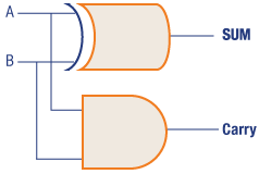
The Half Adder is so called as it adds two input variables, generating a sum and carry outputs; it has no ability to accept a carry-in from a previous adder.
| Input A | Input B | Sum | Carry |
|---|---|---|---|
| 0 | 0 | 0 | 0 |
| 0 | 1 | 1 | 0 |
| 1 | 0 | 1 | 0 |
| 1 | 1 | 0 | 1 |
Figure 16: Half Adder logic diagram and truth table
- 8.2 Full Adder
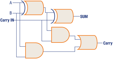
The Full Adder provides the ability to accept a carry-in and is therefore used more commonly when working with multi-bit buses in logic.
| Input A | Input B | Carry In | Sum | Carry Out |
|---|---|---|---|---|
| 0 | 0 | 0 | 0 | 0 |
| 0 | 0 | 1 | 1 | 0 |
| 0 | 1 | 0 | 1 | 0 |
| 0 | 1 | 1 | 0 | 1 |
| 1 | 0 | 0 | 1 | 0 |
| 1 | 0 | 1 | 0 | 1 |
| 1 | 1 | 0 | 0 | 1 |
| 1 | 1 | 1 | 1 | 1 |
Figure 17: Full Adder logic diagram and truth table
Of course, like any logic circuits, there are variations optimized for different applications, including Ripple Carry Adder, Carry Look Ahead, and Carry Save Adders.
We can also use the same adders for subtraction, if we use the twos complement number system to represent signed numbers.
- 8.3 Signed and Unsigned Number Systems
For those not familiar with signed and unsigned binary numbers, we'll very briefly discuss them now. Simply stated, there are several number systems which allow us to represent both signed and unsigned number systems.
Unsigned numbers are the simplest and we can represent a range of 0 to 2n–1, where n is the width of the bus. Unsigned numbers always represent positive numbers. To represent signed numbers, we have a choice of several number systems, the most common being the Sign and Magnitude, Ones Complement, or Twos Complement.
Sign and Magnitude utilizes the left most bit (often called the most significant bit) to represent the sign of the number (0 = positive, 1 = negative), and the remainder of the bits represent the magnitude.
In the Sign and Magnitude system, both positive and negative numbers have the same magnitude; however, the sign bit differs. Due to this it is possible to have both a positive and negative zero within the Sign and Magnitude system.
Ones Complement uses the same unsigned representation for positive numbers as the Sign and Magnitude representation. However, for negative numbers, the inversion (ones complement) of the positive number is used.
Twos Complement is the most widely used encoding scheme for representing signed numbers. Just like Sign and Magnitude and Ones Complement schemes, positive numbers are represented in the same manner as an unsigned number. While negative numbers are represented as the binary number, you add to a positive number of the same magnitude to get zero. A negative twos complement number is calculated by first taking the ones complement (inversion) of the positive number and then adding one to it. The twos complement number system allows subtraction of one number from another by performing an addition of the two numbers. The range a twos complement number can represent is given by: -(2n-1) to + (2n-1–1).
One method we can use to convert a number to its twos complement format is to work right to left, leaving the number the same until the first one is encountered; after this each bit is inverted.
Combinatorial logic circuits are unable to implement functions that require knowledge of their previous inputs or decisions as they contain no memory/storage elements.
In contrast, sequential circuits' outputs are based upon not only current inputs but also previous inputs and decisions. Sequential logic circuits achieve this by using storage elements called flip flops, the simplest of which is the D Type flip flop. The value stored in the flip flop is updated at a regular interval as indicated by the clock signal.
This ability to store states within our logic design allows more complex logic structures to be implemented. It also aids timing as the output of the combinatorial logic circuit must be stable just before the clock is applied to the Flip Flop to store the next value, thereby eliminating glitches. But as we will see this introduces more issues as well, especially when there are multiple layers of logic between flip flops.
- 9.1 Half Adder in a Synchronous Design
In this example, you can see the two-clock cycle delay between the application of an input and the generation of the output. The first clock cycle stores the inputs A and B in the first flip flops. The output of these flip flops will then be passed through the combinatorial logic, in this case, the half adder. The output of the half adder is then stored into the second rank of flip flops and output on the second clock cycle.
- 9.2 Shift Registers and Counters
The three most commonly implemented sequential logic design structures are shift registers, counters, and state machines.
Shift registers in their basic form are a collection of Flip Flops where the output of one flip flop feeds the input of the next flip flop. Signals are then progressed through the shift register on each clock. We can use shift registers for a range of things in our logic design from delays (although there are better ways to implement delays) to metastability synchronizers, as well as conversion between serial and parallel and the generation of random numbers using feedback correctly.

Figure 20: Shift Register and associated timing diagram.
In many designs, we need to time events or introduce delays between the generation or issuing of signals. We do this by using a counter. In this application, we use the flip flops to store the count and combinatorial logic to determine the next value of the count based upon the current value.
The first stage in the development of a counter is to create a simple state diagram which shows the counter behavior.
| Present A | Present B | Next A | Next B |
|---|---|---|---|
| 0 | 0 | 0 | 1 |
| 0 | 1 | 1 | 0 |
| 1 | 0 | 1 | 1 |
| 1 | 1 | 0 | 0 |
Figure 22: Present State, Next State Table for the counter
Once the state diagram is created, we can then create a present state, next state table and extract from it the logic equations to implement the counter. Of course, while the example counts in sequential binary, if we desired, we could have the counter count in gray code, etc.
With the present state, next state table (PS, NS) created, we can then create the logic equations needed to create in combinatorial logic. If necessary we can use Karnaugh-maps, etc. However, for this simple example we can work directly from the present state, next state table.
With the PS, NS table, we create a logic equation for each of the next states, e.g. next A. As such the equations are: Next A = A.B + A.B Next B = A.B + A.B
From these equations we can generate the logic circuit which contains the D Type flip flops and logic gates.
Figure 23: Logic Design for a two-bit counter.
Along with counters, logic designs are often called upon to perform sequence and control-based actions. These actions and sequences are best addressed using a state machine.
- 9.3 State Machines
State machines are logical constructs that transition between a finite number of states, like a counter; however, the path through the states is not sequential. A state machine will only be in one state at a point in time. It will transition between states depending upon several triggers, e.g. inputs or counter values, etc.
Theoretically, state machines are divided into two basic classes: Moore and Mealy. They differ only in how the state machine's outputs are generated.
 Moore: State Machine outputs are a function of the present state only. A classic example is a counter.
 Mealy: State Machine outputs are a function of the present state and inputs. A classic example is the Richards Controller.
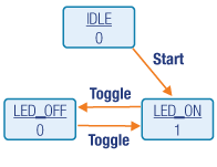
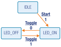
When we are faced with the task of defining a state machine, we will develop a state diagram as we would do for a counter. The state diagram shows the states, inputs, and the transitions between the states and the outputs from the state machine. Figure 24 demonstrates the two types of state diagrams: one for a Moore State Machine (left), the other a Mealy State Machine (right).
Figure 24: State Diagrams for a Moore (left) and Mealy (right) State Machine.
If we were to implement these in logic gates and flip flops we would generate a present state, next state table, as we did for the previous counter example, and then create the logic equations for each of the state variables. The only difference is that, along with the current state, the present state, next state table will also have to consider the inputs and outputs for the state machine.
So far, we have looked at how we create logic designs and implement them with discrete logic gates and flip flops. However, the most common way of implementing a logic design is using a programmable logic device (PLD) such as a Complex Programmable Logic Device (CPLD) or a Field Programmable Gate Array (FPGA). These devices enable the implementation of large logic designs and, depending upon the technology of the device used, they can be reprogrammed in the field.
Programmable logic devices are available in three different technologies:
 SRAM: The FPGA program is stored in an external memory and loaded into the FPGA each time it is powered.
 FLASH: The FLASH architecture of the FPGA also contains the program; no external memory device is needed.
 One Time Programmable (OTP): The FPGA is applied by blowing fuses in the device. Once programmed, it cannot be modified.
Typically, SRAM-based programmable logic is used where high performance is required, while Flash-based devices are used in middle-to-low performance applications. While one time programmable devices are very limited in application, they still remain popular in space applications.
The key to programmable logic is how logic equations are implemented in the device. It is of course very difficult for the device designers to include a range of AND, OR gates, etc. as the number of each gate type will vary with each application. This will result in either many unused gates or a shortage of a needed gate type. Either way it would not be an efficient method for the implementation of a programmable logic device.
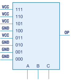
Device manufacturers addressed this challenge in a very smart manner. In place of discrete gates, they use a several input look up table (LUT) which is programmed to implement the combinatorial logic equations. In many respects, this LUT is very similar to a multiplexer. Let's take a quick look at how we can use a LUT to implement logic equations.
Using the same truth table as for the previous example, we can set the LUT inputs to either ground or VCC depending upon the truth table's needs. We can then use the logic equation inputs (A,B,C) to drive the LUT selection inputs to output the correct value for that particular input combination implementing the desired logic equation.
| Input A | Input B | Input C | OP |
|---|---|---|---|
| 0 | 0 | 0 | 0 |
| 0 | 0 | 1 | 0 |
| 0 | 1 | 0 | 0 |
| 0 | 1 | 1 | 1 |
| 1 | 0 | 0 | 0 |
| 1 | 0 | 1 | 1 |
| 1 | 1 | 0 | 1 |
| 1 | 1 | 1 | 1 |
Figure 25: Setting the LUT's Inputs to the Truth Table
Using a LUT inside our programmable device therefore provides the best flexibility to implement a wide range of logic equations.
Of course, we do not want to just implement the combinatorial logic circuits. We also want to implement sequential structures. This means that following the LUT there needs to be a flip flop to act as storage for the combinatorial output such that we can implement sequential structures.
This combination of a LUT and Flip Flop is often called a Configurable Logic Block (CLB). A programmable logic device will consist of many thousands of CLBs. To provide the most flexibility, additional multiplexers will be used to support a wide range of CLB configurations.
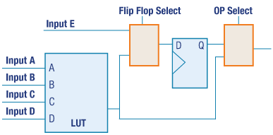
Figure 26: Very Basic Logic Slice
Obviously, modern devices have very complex CLB structures, which include local memory, fast carry inputs, arithmetic functions, and shift registers.
Of course, these CLB's need to be interconnected, which is where the device interconnect comes in, which allows the output of one CLB to be connected to the input of another CLB and eventually to the Input/Output of the device.
This routing can be considered at two elements. First, there is global routing, which distributes global signals such as clocks. These are global specialist routing networks designed to be low skew and support high fan outs. This dedicated clocking network might be further split between truly global routes across the device and several additional regional limited routes to a specific area of the device. For all other signals, the programmable interconnect is used, which connects the CLBs to each other and other specialist functions within the device. To connect CLBs together it uses a switch matrix, which is configured to provide the internal routing between CLBs.
One of the key drivers of programmable logic technology development was the reduction in the cost of transistors. However, interconnect wires also played a role in enabling much larger devices at reduced cost. When we develop programmable logic applications we spend a lot of time and effort optimizing the performance of the design with regards to its routing to ensure we can operate at the desired clock frequency.
To get signals on and off the chip, programmable logic devices also provide IO cells, which are configurable. These enable the device to support a range of single-ended logic standards, e.g. LVCMOS2v4, LVCOM 1V5, etc., Stub Series Terminated Logic (SSTL) as used for High Speed DDR interfaces, and a range of differential standards, including Low Swing Differential Voltage Signaling (LVDS).
Many devices also include complex structures in the IO cells to allow for double data rate signals, source synchronous designs, bus skew correction, and conversion to/from serial. Electrically, the IO can control slew rates, drive strengths and even match the impedance with the transmission line, all of which are controlled by the developer. This means that given the right PHY on the board, using programmable logic, we can achieve any-to-any interconnectivity.
Thanks to the sheer scale of resources offered by programmable logic we cannot any longer design at the gate level like we have done previously. It would simply take too long to develop applications which can leverage the resources provided by the programmable device at the gate level. In the place of developing by using logic equations, we use Hardware Description languages (HDL) such as Verilog or VHDL.
When we work with these languages, we do not describe the logic equations, but rather the desired behavior at the register transfer level (RTL). This allows us to define the functionality of the programmable logic device.
How our description gets translated from our HDL file into the logic equations and implemented in the programmable logic device requires several stages.
| Synthesis |
|---|
| The conversion of the HDL file into logic equations often targeted at the specific resources of the programmable logic device. |
| Placing |
|---|
| Placing of the identified logic cells (LUT, Flip Flops, etc.) into the programmable logic CLBs. |
| Routing |
|---|
| Connecting together the placed CLBs to achieve the required performance. |
Figure 28: Stages to Convert HDL File into Logic Equations
Each stage often requires addition constraints to ensure the desired timing is achieved or the correct IO standards are used.
What developers who are used to using VHDL and Verilog will be familiar with is that not all constructs / commands within a language can be synthesized. Therefore, there is only a subset of language commands and coding structures which can be synthesized into a programmable logic device successfully. The remaining elements of the HDL language which are not synthesizable are used in the verification of the design before we implement it in the device.
This verification is called the development of a test bench which ensures the Unit Under Test (UUT) meets its specification and is suitable for its intended purpose. When it comes to test benching, we have a couple of choices as to how we perform it.
 Functional Simulation only: This checks if the design is functionally correct. It does not include internal device timing delays such as propagation delays, which may affect performance when implemented in the device.
 Gate Level Simulation: This verifies the functionality of the design when back annotated with timing information from the final implemented design. This can take considerable time to perform.

Figure 29: Example Test Bench architecture
Let's look at how we would implement a state machine using the VHDL Language. Learning VHDL itself is a short course; however, we can briefly introduce the basics here.
A VHDL file is split into two distinct elements, the entity and the architecture. The entity defines the input and outputs of the VHDL module and if it is at the top level of the design. It represents the inputs and outputs of the programmable logic device itself.
The architecture defines the functionality and consists of either sequential statements, which are all executed in parallel or processes.
Processes execute sequentially from top to bottom, more like in a traditional programming application. However, there are rules around when signals update during the process. Additionally, each process in the architecture runs in parallel as you are describing logic functions.
|
TYPE state IS (idle, led_on, led_off); SIGNAL current_state : state := idle;
SIGNAL timer : unsigned(24 DOWNTO 0) := (OTHERS =>'0'); SIGNAL toggle : std_logic := '0';
BEGIN
PROCESS(clk,reset) BEGIN IF reset = '1' THEN current_state <= idle; ELSIF rising_edge(clk) THEN CASE current_state IS WHEN idle => op <= '0'; --output is a function of the current state only current_state <= led_on; END IF; WHEN led_on => op <= '1'; current_state <= led_off; END IF; WHEN led_off => op <= '0'; current_state <= led_on; END IF; WHEN OTHERS => op <= '0'; END CASE; END IF; END PROCESS; |
TYPE state IS (idle, led_on, led_off); SIGNAL current_state : state := idle;
SIGNAL timer : unsigned(24 DOWNTO 0) := (OTHERS =>'0'); SIGNAL toggle : std_logic := '0';
BEGIN
PROCESS(clk,reset) BEGIN IF reset = '1' THEN current_state <= idle; ELSIF rising_edge(clk) THEN CASE current_state IS WHEN idle => IF start = '1' THEN current_state <= led_on; END IF; WHEN led_on => IF toggle = '1' THEN current_state <= led_off; END IF; WHEN led_off => IF toggle = '1' THEN current_state <= led_on; END IF; WHEN OTHERS => op <= '0'; END CASE; END IF; END PROCESS; |
Figure 30: VHDL Architecture which shows the implementation of the state machines in the above example
In the above example, the process runs each time the clock or reset is changed. This is defined in the sensitivity list of the process declaration.
In these examples, the reset is asynchronous and used to reset the current state and the output, while the next actions only occur following the rising edge of the clock. Where the state machine progresses through each state depends upon its inputs and current state, moving if necessary to the next state.
What this demonstrates is that, using programmable logic and HDL, we can directly code the state machine or counter from the state diagram and without the need to create the logic equations. Indeed, we let the synthesis tool do that for us.
*Trademark. Xilinx is a trademark of Xilinx Inc. Other logos, product and/or company names may be trademarks of their respective owners.

Shop our wide range of FPGAs, SoCs, EVMs, application specific kits, embedded development boards, and more.
Test Your KnowledgeBack to Top
Are you ready to demonstrate your Essentials of Programmable Logic knowledge? Then take a quick 15-question, multiple-choice quiz to see how much you've learned from this Programmable Devices module.
To earn the Programmable Devices I Badge, read through the module to learn all about Programmable Logic, attain 100% in the quiz at the bottom, leave us some feedback in the comments section, and give the module a star rating.


