Operational amplifiers (or op amps) are one of the most prominent types of linear integrated circuits. They have the property of amplification, and are used for the purpose of signal conditioning, i.e., performing mathematical functions like adding, subtracting, proportioning, integration, and differentiation of the input signals. Low power op amps are an important sub-category of all operational amplifiers. The demand of circuits with reduced power consumption, combined with the fast-growing market of transportable and/or portable equipment have increased the interest in low power op amps. Low power amps can consume 10µA, with some ultra-low power op-amps consuming less than 1µA of current; some are even capable of operating down to 0.5 volts. This learning module will cover the essentials of op amps with a focus on the unique characteristics of ultra low power op amps. The learning module will wrap up with some specific examples of applications for low power op amps.
Related Components | Test Your Knowledge
2. Objectives
Upon completion of this learning module, you should be able to:
- Discuss the characteristics of low power op amps
- Describe the general model of op amp architecture
- Understand various op amp circuit configurations
- Explain some typical applications of ultra low power op amps
3. Overview
The term 'operational amplifier' was coined in the 1940s to refer to a special kind of amplifier that could be configured to perform a variety of mathematical operations. Early op amps were made from vacuum tubes, consuming lots of space and energy. Transistors were commercially developed in the 1960s, which further reduced op amp size to several cubic inches. In subsequent decades, op amps were made even smaller by implementing them with discrete transistors. Today, op amps are monolithic integrated circuits that are not only highly efficient but also consume very small amounts of power.
- 3.1 Definition
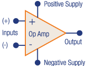
Figure 1: Op Amp Connection Diagram
An op amp is a DC-coupled voltage amplifier IC that uses external feedback components, such as resistors and capacitors, between its output and input terminals. These feedback devices set the "operation" of the op amp. An op amp is typically a three-terminal device, with two high impedance, differential inputs. One of the inputs is called the Inverting Input ( - ) and the other input is called the Non-inverting Input ( + ). A third terminal is the output terminal of the amplifier, which can both sink and source either a voltage or a current.
- 3.2 Categories of Op Amps
The main categories of op amps, based upon application and design requirements, are:
- Precision op amps
- High-speed op amps
- General-purpose op amps
- Low power op amps
- Audio op amps
- Differential op amps
- Power op amps
This learning module will focus on low power op amps, with a special emphasis on ultra low power op amps.
4. Architecture
Op amps are highly compact electronic components, often with hundreds of internal transistors packed onto the die. To illustrate the complexity of a typical op amp, refer to Figure 2, which is the block diagram of the internal architecture of many (but not all) op amps that use a four-stage cascaded block structure.

Figure 2: Op Amp Block Diagram
The input stage is a dual-input, balanced-output, differential amplifier. This stage generally provides most of the voltage gain of the amplifier and also establishes the input resistance of the op amp. The intermediate stage is usually another differential amplifier, which is driven by the output of the first stage. Because direct coupling is used, the dc voltage at the output of the intermediate stage is well above ground potential. Therefore, a level translator (shifting) circuit is used after the intermediate stage to shift the DC level at the output of the intermediate stage towards zero volts with respect to ground. The final stage is usually a push-pull complementary amplifier output stage. The output stage increases the output voltage swing and raises the current supplying capability of the op-amp, and also ensures low output resistance.
5. Op Amp Circuit Configurations
In this section we will discuss the commonly used op amp circuit configurations.
- 5.1 Inverting Amplifier

Figure 3a: Inverting Op Amp
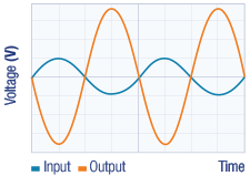
Figure 3b: Inverting Amplifier Input and Output Waveforms
A typical application for an operational amplifier is an inverting amplifier, as shown in Figure 3a. An inverting amplifier takes a positive voltage on the input and outputs an amplified yet inverted signal. In the same manner, the amplifier can also make a negative input voltage positive on the output. (See Figure 3b) In addition, amplification can be selected by choosing the value of the input resistor RI and the feedback resistor RF. The supply voltage must be chosen to be larger than the input voltage range and the desired output range. The limits of the input common-mode range (VCM) and the output voltage swing to the rails (VO) must also be considered.
- 5.2 Non-Inverting Amplifier
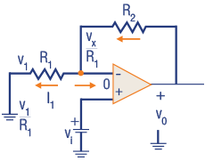
Figure 4: Non-Inverting Amplifier
If a signal is applied to the non-inverting input terminal and feedback is given as shown in the Figure 4, the circuit amplifies without inverting the input signal. Such a circuit is called a non-inverting amplifier. Here the input signal vi is applied directly to the positive input terminal of the op amp, while the other input terminal is connected to ground through R1.
If we assume that the op amp is ideal with infinite gain, a virtual short circuit exists between its two input terminals. Hence the gain of the amplifier is given as:
The gain can be adjusted to unity or more by the proper selection of resistors R2 and R1. Here, the input is applied directly to the terminal, hence input resistance is equal to the input impedance of op-amp, which is infinite.
- 5.3 Difference Amplifier
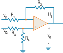
Figure 5: Difference Amplifier
A difference amplifier responds to the difference between the two input signals and ideally rejects signals that are common to both inputs. By combining inverting and non-inverting amplifier configuration and making the two inputs' gain magnitude equal so that the common mode signals are rejected, a difference amplifier can be formed. This is made possible by attenuating the positive input signal to reduce the gains of the positive paths from (1 + (R2/R1)) to (R2/R1) achieved by the voltage divider (R3, R4).
With R1 = R3 and R2 = R4, output voltage can be given as: vo = (R2/R1)(vi2 - vi1).
- 5.4 Summing Amplifier
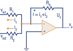
Figure 6: Summing Amplifier
A summing amplifier has two or more inputs, and its output voltage is proportional to the negative of the algebraic sum of its input voltages. A two-input summing amplifier is shown in Figure 6, however, any number of inputs can be used.
Two voltages, vin1 and vin2 are applied to the inputs and produce currents i1 and i2. When the feedback resistor R3 is very large compared to the input resistors, the gain is greater than unity. The expression for the output voltage of a summing amplifier is given as:
vo = (-R3/R) (vin1 + vin2 + vin3 + ... vinn)
Where R is the value of each equal-value input resistor.
- 5.5 Current Source Amplifier
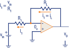
Figure 7: Current Source Amplifier
A consistent current source conveys a load current that remains constant when the load changes. Figure 7 demonstrates a fundamental circuit in which a steady voltage source gives a constant current through the input resistor. Since the inverting input of the op-amp is at virtual ground (0 V), the value of i1 is determined by: i1 = (vin/R1).
Since the internal input impedance of the op-amp is ideally infinite and i1 = iL, then iL = (vin/R1)
When RL changes, iL remains constant, as long as vin and R1 remain constant.
- 5.6 Current-to-Voltage Amplifier
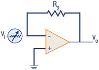
Figure 8: Current to Voltage Converter
A current to voltage converter provides a proportional output voltage by varying the input current. See Figure 8.
In this example, a photoconductive cell like a light dependent resistor is used to sense light level intensity. As the intensity of light changes, the current through the photoconductive cell varies because of resistance change in the cell. This resistance change causes a proportional change in the output voltage.
The equation can be written as Δvo = Δi1R2.
- 5.7 Comparator
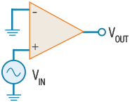
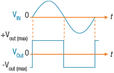
Figure 9: Comparator as a Zero Crossing Detector
A comparator is an op-amp circuit that analyzes two information voltages and produces an output that is either of two states (HIGH or LOW) indicating the relationship between the inputs.
An example of a comparator is a zero crossing detector, which is used to determine the time when the input voltage crosses zero. See Figure 9. Here, the inverting input is grounded, and the input voltage signal is applied at the noninverting terminal. No feedback resistor is connected, and the open-loop voltage gain is very high. This very small difference at the inputs will drive the amplifier into saturation causing the output voltage to the maximum. The zero-level detector used in the previous circuit can be modified to detect positive and negative voltages by using a fixed reference voltage source to the inverting input. This type of circuit can also be used to convert a sine wave into a square wave.
6. Low Power Op Amp Characteristics
As mentioned previously in this learning module, the increased use of portable and battery-powered appliances, such as smartphones and wearable devices, has caused a need for low power electronic components. While electronic components today consume much less power than vacuum tubes of decades ago, low power op amps have been specifically designed to consume little or virtually no power.
The class of low power op amps can be sub-divided into the following categories:
- Ultra low power: less than or equal to 10 µA
- Micropower: 1 µA to 10 µA power consumption per channel
- Nanopower: less than 1 µA power consumption per channel
How are low power op amps designed to achieve such low power consumption? Typically, they operate at lower voltages with lower quiescent current. An electronic circuit that is in a quiescent state for extended periods of time can substantially reduce power consumption, especially at the nanoamp levels.
- 6.1 Process Technology
In addition to designing op amps as low power devices, the technology by which the op amps are processed can enhance their low power characteristics. For example, some of the low power op amps discussed in this learning module have been processed with VIP50 technology. The VIP50 process technology is a silicon-on-insulator (SOI) BiCMOS process with trimmable, highly accurate thin-film resistors which offers a number of advantages over more conventional bipolar or complementary metal oxide semiconductor (CMOS) processes. This process is used to lower power consumption and noise levels in portable handheld devices and medical, industrial, and automotive applications.
7. Low Power Op Amp Applications
Low power op amps are used in a wide variety of circuity, including gas detectors, PIR motion monitors, current sensing circuits, test equipment, signal conditioning circuitry, and all types of portable battery-powered devices. In this section, let's discuss several applications where low power op amps perform an important function.
- 7.1 Battery Monitoring
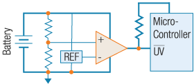
Figure 10: Under-Voltage Detection with a 5-pin Comparator
The need for under-voltage detection in battery powered personal electronics is obvious but how a system engineer provides such detection varies according to the resources available in the system. The most common solution for detecting when a battery voltage gets too low is to use a 5-pin comparator in conjunction with some sort of voltage reference. See Figure 10.
Typically, the comparator and voltage reference are directly powered by the battery if their operating voltage range extends high enough to include the maximum battery voltage. The battery voltage is then reduced with a resistor divider such that the battery voltage will cross the threshold of the voltage reference when the battery reaches a critically low voltage level. Frequently, the output of the comparator is used to alert a microcontroller in the system that the battery level is low. Another option that is commonly exercised is to light an LED in order to provide a visible indication that the battery level is low.
Depending on the usage case, the output level of the comparator may need to be level shifted in order to communicate with a microcontroller or to control a shutdown pin on a DC/DC converter. Level shifting is necessary when the comparator is powered directly from a battery and the device that is monitoring the output of the comparator is operating at a different voltage level. For these applications, a comparator with an open-drain output stage is required.
Comparators with open-drain output stages require a pull-up resistor on their output. When the non-inverting input to the comparator is more positive than the inverting input, the output of the comparator enters a state of high impedance. The pullup resistor now provides the logic high output level for the comparator. Likewise, when the non-inverting input to the comparator is more negative than the inverting input, the output of the comparator creates a low impedance path to ground and sinks current through the pull-up resistor. A low output state alerts the microcontroller that a low battery voltage has been detected.
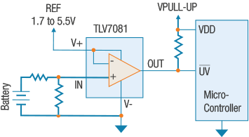
Figure 11: TLV7081 Under-Voltage Detector
A traditional 5-pin comparator is frequently selected to monitor a battery voltage. However, there are alternative solutions available that serve the same function, take up less physical board space, and possess a unique ability of having their input driven even when the operating voltage is zero. One such device is Texas Instrument's TLV7081 which is a 4-pin comparator.
One pin is eliminated by internally connecting the inverting input of the comparator to the positive supply pin. The application of the TLV7081 for an under-voltage detection circuit is shown in Figure 11.
Instead of being powered directly from the battery, the nano-power comparator is powered directly from a voltage reference that exists in the system. The input to the comparator is allowed to operate above and below the reference voltage due to the unique analog front end of the TLV7081. When the battery voltage is above the reference threshold, the output of the comparator is high and when the battery drops below the threshold of the reference, the output of the comparator goes low (See Figure 12). For simplicity, the integrated hysteresis of the comparator is not shown in the timing diagram. Integrated hysteresis is helpful in avoiding glitches at the comparator output when operating in noisy environments or when the input voltage changes thresholds very slowly. An open-drain output configuration allows the output logic level of the comparator to be level-shifted to match the logic level of the receiving device.
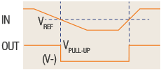
Figure 12: Timing Diagram
In addition to saving board space, the 4-pin comparator has other circuit advantages. First, the battery input can be connected to the input of the comparator even if the reference voltage is not powered. Most comparators have ESD protection diodes on the input that prevent the input from being driven when the supply to the comparator is disabled. This is possible in the TLV7081 because the comparator's input stage is designed to accept voltage levels independent of the operating voltage applied to the supply pins. Being able to leave an input voltage such as a battery connected to the input of the comparator even when the comparator is powered down eliminates any power supply sequencing concerns. Moreover, it provides a secondary means for saving power.
Comparators such as the TLV7081 are nano-powered, but for applications such as energy harvesting applications where total power consumption needs to drop below 100nA when a battery voltage drops to dangerously low levels, devices such as the TLV7081 can be power cycled by a microcontroller GPIO pin or a nanotimer device. In Figure 11, a GPIO pin of the microcontroller is used as the supply voltage for the comparator. Since the input stage's input voltage range is independent of the supply voltage, the battery voltage can remain connected to the comparator input without any negative impact to the circuit.
A second advantage to the 4-pin comparator is the performance improvement that results when powered directly from a reference. Since the reference voltage is well regulated, there will be little or no comparator offset change due to the operating voltage changing (there will be no noticeable PSRR error contribution).
In the case of the 5-pin comparator configuration, the comparator is directly powered by the battery that will sag over time. The sagging of the battery will have an impact on the threshold voltage of the comparator due to a finite power supply rejection ratio.
For battery powered systems requiring under-voltage detection, 4-pin comparators such as the TLV7081 offer several advantages over the traditional 5-pin options. The smaller PCB footprint, removal of power supply sequencing concerns, low-power consumption, and improved threshold accuracy due to operating directly from a reference make 4-pin comparators a logical choice for systems requiring under-voltage detection.
- 7.2 Oxygen Gas Sensor
Heightened accuracy and speed in an op amp has a direct relationship with the magnitude of its power consumption. Decreasing the current consumption decreases the gain bandwidth; conversely, decreasing the offset voltage increases the current consumption. Many such interactions between op amp electrical characteristics influence one another. With the increasing need for low power consumption in applications like wireless sensing nodes, the Internet of Things (IoT) and building automation, understanding these trade-offs has become vital to ensure optimal end-equipment performance with the lowest possible power consumption. Let's see how this line of reasoning plays out in an application example. But first, let's review some op amps basics again.
DC gain
The closed loop gain equations for classic inverting and noninverting op amps are:
Inverting Op Amp: ACL = - RF/R2 = - VOUT/VIN (Equation 1)
Non-Inverting Op Amp: ACL = 1 + (RF/R2) = (VOUT/VIN) (Equation 2)
where ACL is the closed-loop gain, RF is the value of the feedback resistor and R2 is the value of the resistor from the negative input terminal to signal (inverting) or ground (noninverting). These equations are a reminder that DC gain is based on resistor ratio, not resistor value. Additionally, the "power" law and Ohm's law show the relationships between resistor value and power dissipation:
P = VI (Equation 3) where P is the power consumed by the resistor, V is the voltage drop across the resistor and I is the current through the resistor.
For nanopower gain and voltage divider configurations, P=VI tells you that, in order to minimize power dissipation, you need to minimize the current consumption by the resistor. The below equation helps you understand the mechanism to do that:
V = IR (Equation 4) where R is the resistor value.
Using these equations, you can see that you must choose large resistor values that provide both the gain you need while minimizing power dissipation (and therefore power consumption). If you don't minimize current through the feedback path, you'll lose the benefit of using nanopower op amps.
Once you've determined what resistor values will meet your gain and power-consumption needs, you'll need to consider some of the other op amp electrical characteristics that will affect the accuracy of signal conditioning. Summing several small systemic errors inherent in nonideal op amps will give you the total offset voltage. The electrical characteristic, VOS, is defined as a finite offset-voltage number between the op amp inputs, and describes these errors at a defined bias point. Please note that it does not describe these errors across all operating conditions. To do that, you must consider the gain error, bias current, voltage noise, common-mode rejection ratio (CMRR), power-supply rejection ratio (PSRR) and drift. Covering all of these parameters is beyond the scope of this learning module, but let's look at VOS and drift—and their influence in nanopower applications—in a bit more detail.
Real-world op amps exhibit VOS across their input terminals, which can sometimes be a problem in low-frequency (close to DC) precision signal-conditioning applications. In voltage gain configurations, the offset voltage will gain up along with the signal being conditioned, introducing measurement errors. In addition, the magnitude of VOS can change over both time and temperature (drift). Therefore, in low-frequency applications requiring fairly high-resolution measurements, it's important to select a precise (VOS ≤ 1mV) op amp with the lowest possible drift.
The below equation calculates the worst-case VOS over temperature:
| VOSmaxtemp | = | VOS(25°) | + | TCVOSmax | x Application Temp Range (Equation 5)
Now we're ready to discuss our example, using two-lead electrochemical cells. For two-lead electrochemical cells which often emit very small signals of low frequency, and are used in diverse portable sensing applications like gas detection and blood glucose monitoring, choose a low-frequency (<10kHz) nanopower op amp.
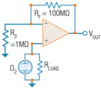
Using oxygen sensing as the specific application example, assume that the maximum concentration of the sensor outputs 10mV (converted from current to voltage by a manufacturer-specified load resistor, RL) and the full-scale output of the op amp is 1V. Using Equation 2, you can see that ACL needs to be 100, or RF needs to be 100 times larger than R2. Choosing values of 100MΩ and 1MΩ, respectively, gives you a gain of 101, and these resistor values are large enough to limit current and minimize power consumption.
To minimize offset error, the LPV821 zero-drift nanopower op amp is a good choice. Using Equation 5 and assuming an operating temperature range from 0°C to 100°C, the worst-case offset error introduced by this device will be: VOStemp_LPV821 = | 10µV | + | 0.08(µV/°C) | x 100°C = | 18µV |
Another good choice is the LPV811 precision nanopower op amp. Using its data sheet to gather the necessary values plugged into Equation 5 gives you: VOStemp_LPV811 = | 370µV | + | 1(µV/°C) | x 100°C = | 470µV |
If you were to use a general-purpose nanopower op amp like the TLV8541 instead, those values would result in: VOStemp_TLV8541 = | 3.1mV | + | 0.8(µV/°C) | x 100°C = | 3.18mV |
As you can see, the LPV821 op amp is the best choice for this application. With 650nA of current consumption, the LPV821 can sense changes in the output of the oxygen sensor down to 18µV or lower, and introduces a maximum offset gain error of only 2.3mV. When you need both extreme precision and nanopower consumption, a zero-drift nanopower op amp will provide the best possible performance.
- 7.3 Low-side differential current measurement
Designers perform current sensing for system protection and monitoring by placing a very small "shunt" resistor in series with the load, across which there's a current-sense amp or an op amp. Purpose-built current-sense amps are exceptionally good at sensing current, but in cases where power consumption is most important, a precision nanopower op amp is a good alternative.
There are two positions in which you can place the shunt resistor with respect to the load: between the load and the supply (High side), or between the load and ground (Low side).
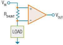
High-side Current Sensing
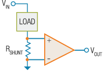
Low-side Current Sensing
Figure 14: High-side and Low-side Current Sensing
In both cases, to sense current with a known resistor value, the op amp measures the voltage across the terminals of the shunt resistor. Using Ohm's law (Equation 1), you can determine the current consumption: V = IR (Equation 1) where V is the voltage, I is the current and R is the resistance.
Choose the shunt resistor and op amp so that they will have minimal impact on the circuit's behavior. In selecting a resistor, there are two factors driving the need for a low-value resistor:
- Keeping the voltage drop across the resistor as small as possible so that the load's negative terminal is as close to ground as possible in low-side sensing, or as close to the supply as possible in high-side sensing.
- Keeping power dissipation low. Equation 2 shows that, since you are measuring current and it is therefore the independent variable, the resistance should be as small as feasible: P = I2R (Equation 2).
A point of clarification: Since you are measuring current rather than trying to minimize current, you need to minimize the value of the resistor to also minimize power dissipation—this is the opposite thought process of managing power dissipation in DC gain configurations.
Ultra-low-power current-measurement techniques are useful in end equipment like power bank battery charging and monitoring, mobile phone battery charging and monitoring, and even ensuring the correct functioning of industrial Internet of Things applications.
So just how low can you go when selecting resistor values? Simply put, the voltage drop across the resistor should be larger than the offset voltage of the op amp you're using.
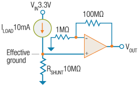
Figure 15: Low-side differential current measurement
Let's say that you want to perform low-side differential current measurement (Figure 15) to ensure that there is neither a short nor an open connection in your system. For the purpose of simplicity, let's choose easy numbers for this example and ignore parameters like resistor tolerance.
The supply voltage is 3.3V. The system draws a maximum of 10mA when operating correctly, and you don't want the effective ground that the load sees to be any higher than 100µV. The first thing you'll realize is that your shunt resistor must exhibit a voltage drop (due to current) less than or equal to 100µV.
If you use Equation 3 to determine the maximum shunt resistance: RSHUNT = 100µV/10mA = 10 mΩ (Equation 3).
Your effective ground will be 100µV, as shown in Equation 4: Effective ground = 10mΩ x 10mA = 100µV (Equation 4).
You must choose an op amp that is able to detect changes in this voltage drop, which indicates a fault condition. Since the system is in a normal operating condition when the load current is within ±10% of its typical value of 10mA, your op amp will then be able to detect the change in voltage across the sense resistor when the current changes by at least 10%.
When there is a fault condition (such as an open circuit, a brownout from low current, or a short-circuit or brownout from high current), Equation 5 expresses the change in current (IΔ) as: IΔ = 10mA x10% = 1 mA (Equation 5).
Equation 6 calculates the resulting change in voltage drop across VSHUNT: VΔ = 1mA x10mΩ = 10µV (Equation 6).
In this example, I would choose the LPV821 zero-drift nanopower amplifier. Its zero-drift technology enables a maximum offset voltage of only 10µV, allowing it to detect the fault condition. Zero-drift op amps are ideal for high accuracy (<100µV) measurements. Additionally, the LPV821 is also a nanopower amplifier, which means you can leave it always-on, and it will continue to deliver accurate current-sense measurements with very little impact to the system power budget.
- 7.4 Two Pole Sallen-Key Low Pass Filter
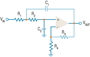
Figure 16: Two Pole Sallen-Key Low Pass Filter
The LMV551 is a high-performance, low-power operational amplifier implemented with TI's VIP50 process technology. This ultra-low power amplifier has unity gain stable and provides an excellent solution for ultra-low power applications requiring a wide bandwidth. With a wide unity gain bandwidth of 3 MHz, low input referred noise density and an excellent BW to supply current ratio, it is well suited for low-power filtering applications. Active filter topologies, such as the Sallen-Key low pass filter shown in Figure 16 can be used to design a wide variety of filters (e.g., Chebyshev, Butterworth or Bessel).
For best results, the amplifier must have a bandwidth that is eight to ten times the filter frequency bandwidth. Failure to follow this guideline can result in phase shift of the amplifier and premature roll-off. The Sallen-Key topology, in particular, can be used to attain a wide range of Q, by using positive feedback to reject the undesired frequency range.
The LMV551 is targeted for low power operation. The above resistor values are assumed for a standard power application. To save power, both quiescent and dynamic, the values of the resistors can be increased. The largest consumer of power is the gain setting feedback resistors R3 and R4, as these are DC coupled and represent a constant DC load to the amplifier. If the output is biased at 2.5 V, then 2.5 V / (22.6 k + 2.49 k) = 99.6 µA is flowing through the feedback network. This is significantly more than the 37uA quiescent current of the amplifier alone! Increasing the size of the feedback resistors by a decade from 22.6k to 226k, the current in the feedback network can be reduced down to 9.9uA.
Increasing the resistor values requires a proportional decrease in the values of the capacitors. If a resistor value is increased 10×, then the corresponding capacitor value must be decreased 10×. However, note that increasing the resistor values increases the contributed noise, and decreasing the capacitors to small values increases the sensitivity to stray capacitance.
A decision must be made also about scaling the filter components (R1, R2, C1 & C2). R1 and R2 are AC coupled to the output, so the only DC current flowing through these resistors is the input bias current of the LMV55x (typically 20 nA). However, large AC currents can flow through C2 and C1 during large signal swings.
Scaling the filter components also reduces the peak AC signal currents. If the AC signals are expected to be large (several Vpp) and frequent, then scaling the filter values may be beneficial to overall power consumption. If the expected AC signals are small, it may not be worth the noise tradeoff to scale these values. Because the LMV55x has a bipolar input, to maintain DC accuracy, the equivalent resistance seen by each amplifier input should be equal to cancel the bias current effects.
To maintain DC accuracy through bias current cancelling, the following relationship should be maintained: (R1 + R2) = (R3 // R4)
By changing the value of any of the filter components (R1, R2, C1 & C2) in the schematic tab, the program automatically recalculates and scales these components. Conversely, changing the gain feedback components (R3 or R4) also causes the other feedback resistor to scale. The feedback resistor values can be 'seeded' and scaled appropriately, as long as the original feedback resistor ratio is maintained.
8. Other Design Considerations
We will wrap up this learning module with some general guidelines for op amp circuit design, as well as other things that are good to know when you are designing with op amps.
- 8.1 Open Loop
It is possible to use the real operational amplifier in an open loop configuration, but control and stability problems are encountered due to the high open loop gain (x105 typically at DC). Random noise from the input circuit and noise generated within the operational amplifier itself plus any variations in amplifier characteristics due to temperature change or aging components, are all multiplied by open loop gain. (Source: Texas Instruments: Handbook of Op Amp Applications)
- 8.2 Closed Loop
When feedback is used around an operational amplifier, the closed loop gain of the circuit is determined by a ratio involving the input and feedback impedances used. If the closed loop gain called for by the feedback configuration is greater than the open loop gain available from the operational amplifier for any particular frequency, closed loop gain will be limited to the open loop gain value.
- 8.3 Coupling
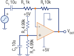
Figure 17: Example of Inverting Op Amp with AC Coupling
AC coupling: In AC coupling, a capacitor is used to filter out the DC signal component from an input signal with both AC and DC components. See Figure 17.
The voltage gain for this circuit is calculated assuming that the input capacitor C1 is shorted. In such a case, the formula would be: Gac = - (Rf/R1)
The voltage divider R1 C1 and the input RC network sets the lower cutoff frequency for the circuit. It is desirable to set fl as low as possible. Increasing R1 or C1 will decrease this frequency further, but this will also increase the transient startup for this circuit. Furthermore, choosing a large value for R1 will increase noise.
DC coupling: DC coupling does not affect the signal at all. Everything that goes in comes out again.
- 8.4 Input and Output Limitations
An op amp has a limitation on its input voltage range and output swing. These parameters are set by the op amp manufacturers. To operate the op amp into the linear region, the designer should ensure that the input signal not exceed the limit set by the manufacturer.
- 8.5 Power and Temperature
Not all the energy supplied by the power source gets used in the amplification process. Some energy is lost in the operation of the device, which is commonly known as power dissipation (PQ). It is determined by the quiescent current that flows through the device.
PQ = IQ x Vs (Where IQ = quiescent current and VS = total supply voltage)
This power dissipation results in an increase of the device temperature, which needs to be managed to ensure the proper performance of the device. Most ICs provide internal thermal protection. It is preferred to use an adequate heatsink for thermal dissipation and to control the temperature within the desired limits to avoid unnecessary cut offs.
- 8.6 Bandwidth
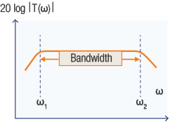
Figure 18: Typical magnitude response of an amplifier.
Figure 18 shows the magnitude response of an amplifier. ( |T (ω)| is the magnitude of the amplifier transfer function.) It indicates that the gain is almost constant over a wide range of frequencies, roughly between ω1 and ω2. Signals whose frequencies are below ω1 or above ω2 will experience lower gain, with the gain decreasing as we move farther away from ω1 and ω2.
The band frequencies over which the gain of the amplifier remains constant (usually with a 3dB maximum deviation) is called the amplifier bandwidth. Normally, the amplifier is designed so that its bandwidth coincides with the spectrum of the signals it is required to amplify. If this were not the case, the amplifier would distort the frequency spectrum of the input signal, with different components of the input signal being amplified by different amounts.
- 8.7 Slew Rate
The slew rate is the maximum rate of change of output voltage with respect to time. It's usually specified in volts per microseconds: SR = (dVo/dt)V/µS
The slew rate is caused by current limiting and the saturation of internal stages of an op amp when a high frequency, large amplitude signal is applied.
- 8.8 Common Mode Rejection Ratio
When the same input voltage is applied to both input terminals of an op amp, it is operating in a common mode-configuration. This common-mode voltage (vcm) can be AC, DC, or a combination of AC and DC. Ideally, an op-amp amplifies the difference of the input voltages; therefore, no common-mode output voltage should appear at the output. The common mode gain is calculated with the following: Acm = (Vo cm/Vcm)
Op-amp manufacturers usually list a common-mode rejection ratio CMRR. Generally, it can be defined as the ratio of the differential gain AD to the common-mode gain Acm that is, CMRR = (AD/Acm) Where AD is equal to internal gain A of the op-amp.
Generally, the CMRR value is very large and is therefore usually specified in decibels (dB): CMRR (dB) = 20 log (AD/Acm)
- 8.9 Power Supply Rejection Noise
It is the ratio of the variation or change in power supply voltage and the delta differential output created by the variation. Ideally, PSSR should be infinite and is measured in decibels indicating the ability of the circuit to provide a stable and accurate output despite supply variations. Though primarily measured in DC conditions, it is also applied and defined at various frequencies.
- 8.10 Linear and Non-linear Response
For the amplifier to work in the linear region, the following design issues should be considered:
- Look for an amplifier with high open loop gain, low intrinsic distortion, and high slew rate.
- For voltage feedback op-amps, gain bandwidth products in the gigahertz range may be required to provide enough gain to reduce distortion significantly in the range of 10 to 100 MHz.
- Current feedback operational amplifiers have much higher slew rates than voltage feedback operational amplifiers. For this reason, current feedback op-amps can provide a lower distortion in high-frequency applications.
- For higher gain, applications use decompensated operational amplifiers. Decompensated operational amplifiers sacrifice stability at a lower gain for the higher gain-bandwidth product, higher slew rate, and lower noise.
Some of the op-amp applications are nonlinear and it is useful to operate op-amps in the nonlinear region. Some examples include an op-amp comparator, Schmitt trigger, half wave rectifier, and more.
- 8.11 Input Offset Voltage
It is possible that an op amp's output voltage may not be zero even with zero input voltage. This is due to the unavoidable imbalances inside the op-amp. One may have to apply a small voltage at the input terminals to make the output voltage zero. This voltage is called input offset voltage, Vios.
- 8.12 Input Bias Current
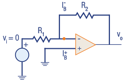
Figure 19: Input Bias Current
Where Vo = 0V
The op-amp's input is a differential amplifier, which may be made of BJT or FET. In either case, the input transistors must be biased into their linear region by supplying currents into the bases by the external circuit. In an ideal op-amp, we assume that no current is drawn from the input terminals. However, practically speaking, the input terminals conduct a small value of DC current to bias the input transistors. The base currents entering into the inverting and non-inverting terminals are shown as I-B and I+B respectively in Figure 19. Even though both the transistors are identical, I-B and I+B are not exactly the same due to internal imbalances between the two inputs.
- 8.13 Low Distortion Design
Distortion noise should be minimized from the design, both at the output as well as at the input stages, along with external sources that may induce noise. Distortion sources from the op amp's input stage are suppressed in the following ways:
Minimize Op Amp Input Differential Voltage (VDIFF)
- Reduce output voltage (not usually an option)
- Reduce gain (may not be an option)
- Maximize Open Loop Gain (AOL)
- High supply voltages
- Select parts with proper Gigahertz Bandwidth (GBW)
- Prevent Input Crossover Distortion
- Observe input CM voltage range in the datasheet
- Use inverting amplifier topology
- Use zero-crossover distortion op amps: OPA320, OPA322, OPA365
- Prevent Common-Mode Impedance Effects
- Use inverting amplifier topology
- For non-inverting amplifiers match impedances at both op-amp inputs
- Select parts with dielectrically isolated JFET inputs: OPAx140/x141/164x, OPA827, BB DiFET OPAs (OPA627, OPA2107, etc.)
Reduce distortion sources from an op amp's output stage
- Limit output loading
- Increase feedback resistor values and load resistance
- Improve crossover distortion performance
- Increase output voltage swing (not usually an option)
- Bias output stage into class A with a resistor to the supply (increases power consumption)
- Stay away from clipping regions
- Use inverting amplifier topology
- Maximize supply voltage
- Confirm linear swing range in the datasheet (AOL test conditions)
- Composite Amplifiers
- Place a buffer inside the feedback loop of another amplifier
- Increases the amount of loop gain around the output stage
- Place a buffer inside the feedback loop of another amplifier
Reduce distortion from external sources
- Minimizing distortion from power supplies
- Choose op amps with high PSRR in the desired passband
- Design power supplies to limit their output impedance
- Bulk decoupling capacitors, linear regulators, short PCB traces
- 8.14 Electrostatic Discharge
Some materials tend to become positively charged and others become negatively charged. Whenever two items with a charge imbalance are brought in close proximity or in contact, electricity flows between the two objects, which is called electrostatic discharge (ESD). ESD can show up as a visible spark and often has voltage levels in the thousands of volts. ESD problems can be avoided by using good PCB layout techniques, e.g., eliminating circuit loops, avoiding long signal traces, avoiding running critical signal traces (clocks, resets, etc.) near PCB edges, and protecting all external connections with TVS diodes.
- 8.15 Electrical Overstress
Electrical overstress (EOS) occurs when a voltage is applied at the inputs of the op amp that exceeds the absolute maximum rating of the op amp. The EOS may stay for a much longer time, though the excess voltage may be just marginally high. This tends to draw very high currents from the device, resulting in increase in temperature and failure of the Op amp. Transient Suppressor (TVS) diodes are used to protect the op amp from EOS.
To extend the information covered in the main module, a supplementary section discusses the types of related components used in op amps circuits. Click here to explore.
*Trademark. Texas Instruments , and TI are trademarks of Texas Instruments Inc. Other logos, product and/or company names may be trademarks of their respective owners.
Shop our wide range of low power operational amplifiers, including ultra low power, micropower, and nanopower op amps, as well as associated development boards.
Test Your Knowledge
Op Amps I

Are you ready to demonstrate your Low Power Op Amps Essentials knowledge? Then take a quick 15-question, multiple-choice quiz to see how much you've learned from this learning module.
To earn the Essentials of Low Power Op Amps I Badge, read through the learning module, attain 100% in the quiz at the bottom, and leave some feedback in the comments section.

