One of the core skills of any electronics engineer is the ability to design circuit cards or boards, as they are often called. These circuit boards can contain FPGAs, Programmable SoCs, DSPs, Microcontrollers, Processors and supporting peripherals, which enable a flexible software-defined solution. Designing a successful circuit board requires several considerations; it's not as easy as one would think. In this Essentials learning module, we will explore how to create circuit boards for embedded systems.
2. Objectives
By the end of this essentials course you will understand:
 The importance of engineering governance and requirements
 The key role that requirements and interfacing play in successful development
 The different stages of design involved in creating a circuit board
 The importance of design for manufacture and test
Additionally, you will also understand the stages of board design, and how to judge the design's maturity as it moves from one stage to the next.
Engineering governance defines the process followed from an initial concept, to delivery of the circuit board, and on through its eventual disposal. In essence, it defines the entire engineering approach to the the board's development project.
The complexity of the engineering governance process at most engineering companies will depend upon the targeted application of the board and the company size. Enforcement of the engineering governance process is normally the responsibility of a lead or chief engineer.
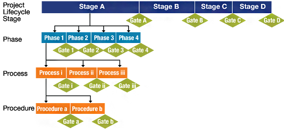
At the highest level, the engineering governance structure will split the design and development of the circuit board into several stages. As these stages progress, so too does the maturity of the design. Typical stages will include:
 Requirements Capture: Capture the requirements for the application at hand
 Preliminary Design: Preliminary architectural design, interface definition, component selection, and mechanical diagrams
 Design: Creation of the schematics and layout
 Manufacture and Test: Manufacture and test of the design to ensure it meets the specified requirements
 In-life support & end of life: Support in the field and safe disposal as the product's life ends
Typically, between each of these stages will be a major design review which assesses the design maturity, identifies technical risks, and allows the design to progress on to the next stage or not.
To ensure successful stage completion, there exist processes and procedures which outline how to perform specific elements of the design for that stage. For example, the schematics' review procedure would detail how to review a schematic design. This procedure may include a checklist with several questions the designer has to answer about their design. These checklists are then used to demonstrate the maturity of the design in order to move from one stage to the next at the appropriate design review.
- 3.1 Engineering Governance Structure
For a typical project, there will be the following major design reviews between stages:
 KO (Project Kick Off): Alignment of the engineering delivery team with the goals and timescales of the project
 SRR (System Requirement Review): Review and freezing of the requirements for the design
 PDR (Preliminary Design Review): Review of the architectural design
 CDR (Critical Design Review): Review of the schematics, design analysis, and layout of the design.
 MRR (Manufacturing Readiness Review): Review of the manufacturing data pack
 TRR (Test Readiness Review): Review of the test requirements, availability of test equipment to begin the test campaign
 TRB (Test Review Board): Review of the test results against the requirements and product release, if successful
As part of the engineering governance program, the circuit board or final assembly may be required to undergo regulatory compliance testing (e.g. FCC, CE, IEC61508, etc.). The need to gain regulatory compliance should be accommodated within the engineering governance structure.
Figure 1: Stages of Project Lifecycle
One reason many projects fail is because they do not have a clear, unambiguous, and achievable set of requirements. Having such a set of requirements is the starting point for all projects, and this holds true for the circuit board we wish to design.
The requirements landscape can be complex; in a complex system, it is likely that there will be multiple levels of hierarchy to the requirements, ranging from the system requirements down to circuit card, software, and FPGA requirement sets.
The number of requirements placed on a system can have a significant impact on the overall development timescales and cost. It is, therefore, good practice to generate a requirement set which is concise and contains requirements that are:
 Necessary: Success cannot be achieved without this requirement
 Verifiable: You must be able to ensure the requirement can be implemented via inspection, test, analysis, demonstration or read across
 Achievable: Technically possible, despite the constraints
 Traceable: Can be traced across the requirement hierarchy; for example, lower level requirements trace to higher level requirements
 Unique: Prevents contraction between requirements
 Simple and Clear: Each requirement specifies one function
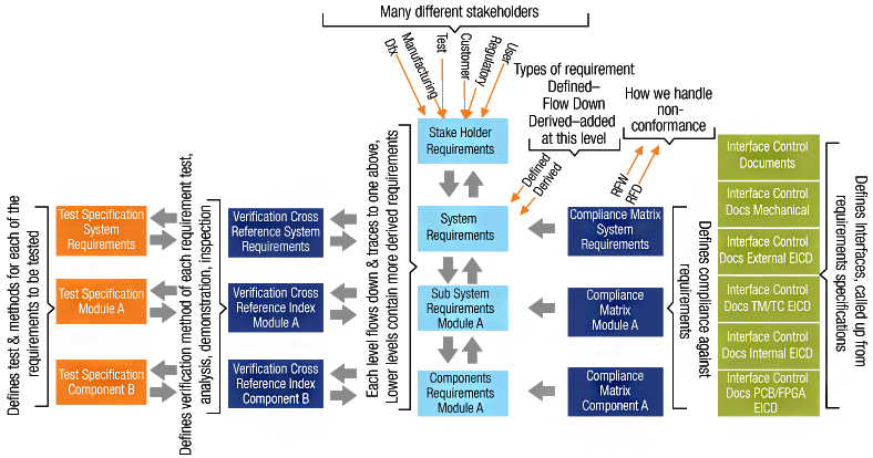
Of course, the requirements are just the start of the story. We can then proceed to create compliance matrices which demonstrate if we will be compliant with the requirements placed on the board or not.
Then, we can create verification cross reference indices which define how each requirement is going to be verified. Examples of verification methods include test, analysis, read across or demonstration.
Once it is known how each requirement is to be verified, test specifications can be generated, thus completing the requirements set.
If there are any issues with the requirements (e.g., non-compliance), we can raise a request for deviation with the customer during the design phase or a request for waiver if the issue arises during the test phase.
Figure 2: Issues with Engineering Requirements
Engineering budgets are a response to requirements and are contained in the requirements specification. An engineering budget allocates portions of the overall target defined by a system requirement to sub-systems in the design, providing clear guidance and targets to the designers. Typical budgets would be power budgets which allocate the available power to different sub systems and mass budgets, which allocate the overall mass requirements to sub-systems.
Once we fully understand what we are being requested to design, we are then able to move forward and develop the architecture of the solution.
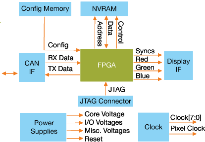
The architecture is a response to the requirements, and it identifies the major components of the design at a block diagram level. There will be several elements to the architecture itself, which include:
 Overall Architecture: The overall solution architecture at the highest level
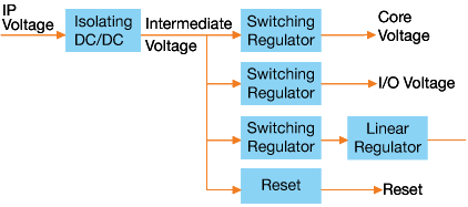
 Power System Architecture: The architecture of the power system outlining how the required voltage rails are generated
 Clock and Reset Architecture: The clock architecture of the solution, which is especially important for mixed signal designs
Once completed, the architecture can then be presented to the customer for agreement as part of the preliminary design review.
The overall architecture will provide an indication as to the major components required for the design, and provoke discussion regarding the necessary tradeoffs which must be made to develop an architecture compliant with the requirements. Such tradeoffs may include the use of separate processors and FPGAs or combined SoCs. The architecture also provides the size and type of memories required, along with defining the interfacing both internally and externally of the system.
Figure 3: Example of an Architectural Diagram for a FPGA based system
Of course, the power system and clock & reset architecture require a little more detail on the component selection, so they may be appropriately designed.
During the architecture phase, it is also common to perform the device selection, and to identify the main components used in the design (e.g., Processors, FPGAs, Memories, Mixed signal converters, etc.).
Once these components have been identified, we are able to understand the power and clocking requirements from the data sheets and create the necessary architecture. In many cases, spreadsheets and applications will be provided which enable us to identify the power requirements. These power demands can then be used to correctly determine the power architecture, ensuring it complies with all available engineering budgets.
Figure 4: Example of a Power Architecture
One of the major impacts on the design is the identification and selection of components to be used. This includes not only the digital and analog integrated circuits, but also the discrete and passive components, especially if there are challenging analog requirements.
Selecting the components will be based on not only the desired performance, but also packaging, quality level, availability, and unit price. Typically, component selection involves reading and analyzing many different datasheets from a range of vendors. This enables us to create a short list of candidate components, and then perform a comparison between the candidates to identify the final device to be selected.
It is during this phase that picking up the phone and talking to field application engineers about the candidate components can be very useful, especially if there are corner cases which need to be explored, to ensure suitability for the design. In this case, prototyping and testing with development boards can be very useful in identifying suitable components, as well as reducing the technical risk as the design progresses.
When identifying components, we may desire to select components with a second source, if possible, in order to help mitigate the risk of obsolescence. However, this is increasingly difficult for high performance components, which tend to be single source only.
During the component selection process, we must also be cognizant of internal company component approval processes which are used by companies to ensure components proposed for a design align with the purchasing, manufacturing, and availability constraints.
To help select the final component from the candidate list, we can create a Pugh Matrix. A Pugh Matrix starts by defining a set of criteria which are then scored and summed. This gives each option a ‘final score' which can then be ranked, allowing our final component list to be created.
The board's interfaces represent an area of risk. This risk arises as the interfaces include multi-disciplinary factors such as Electronic and Mechanical Design, or arise due to the ability of the board to externally interface with other systems. To mitigate the risk of incorrect interfaces, we use what is commonly called an Interface Control Document (ICD). These ICDs enable us to clearly define the different interfaces within our system, covering a range of disciplines. As such, they will cover areas such as:
 Mechanical ICD: A mechanical ICD will define the mechanical aspects of the design. This will include not only the external dimensions and tolerances, but also additional requirements such as finishing, emissivity, and flatness. Depending upon the complexity of the solution, internal mechanical ICDs may simply address how the circuit board mounts within the enclosure, or how several circuit boards and a back plane are contained within the enclosure. Of course, these internal ICDs will also include mounting points, keep-out areas, and mechanical bracing and thermal paths for the circuit boards.
 Thermal ICD: A thermal ICD will define the thermal interfaces of the system. This will include the thermal conductivity between the enclosure and the mounting points, along with any additional thermal management methods. These additional thermal management methods may include forced air cooling, conductive paths, or liquid cooling. The thermal ICD enables the system designers to understand the thermal environment, so they can design a system which can operate within it. The thermal ICD will also be very useful when (or if) it comes to determining the part stress analysis and reliability figure.
 Electrical ICD: An electrical ICD will define all the electrical interfaces of the system. Often, this will be split into an external electrical ICD and an internal electrical ICD. The electrical ICDs will define the power supplies, signal interfaces, and grounding. Obviously, when working with electrical interfaces, we should try to work with industry standard interfaces such as Ethernet, RS232, USB, etc., depending upon the needs of the system. Along with standard interfaces, we should use standard connectors such as FPGA Mezzanine Card (FMC), Arduino Shield, and Pmod wherever possible, depending upon the needs of the application.
Once the interfacing, requirements, and architecture are understood, we are able to hold the preliminary design review to assess the maturity of the design and its suitability to progress on to the next stage of detailed implementation.
Schematic design is the traditional stage you think about when it comes to designing a circuit board. However, as we have seen, there are several stages which come before we start creating the schematics if we want to be successful.
It is at the schematic stage that we capture the behavior of the electronic circuits. To be able to correctly capture the desired behavior in the schematics, we must first have all the chosen components drawn up and added to the library. Drawing up the components will provide both the schematic symbol and the layout footprint.
When creating the schematic, we want to make it easy to review and minimize duplication as such if possible, so we want to:
1) Create a hierarchical schematic which aligns with the architecture
2) Create reuse-modules which enable easy duplication if the circuit is repeated in the design (e.g., FPGA modules or power modules)
During the schematic design stage, we must also ensure that not only do we implement the functionality desired but also ensure we implement structures for test. These structures include:
 JTAG / Boundary Scan: Provides the ability to program devices and perform manufacturing connectivity testing of the board using boundary scan
 Test Points: Provide test points on the voltage rails, clocks, and resets. It is a good idea to provide a ground test point close to the measurement test point. If voltage rails are being measured, a protection resistor can be placed between the rail and the test point to limit current if the rail is accidentally shorted, preventing damage to the board. When measuring clocks, we also need to be able to ensure the clock signal is properly terminated and the test point does not affect the clock signal. In this case, a spare output on a clock buffer can be terminated and used to provide a test point which is isolated from actual clock signal.
Along with the testability of the design, we also need to begin to consider the signal and power integrity of the design. Ensuring signal integrity requires the use of the correct termination scheme for the signal. One key aspect of ensuring the signal integrity is that it is not the frequency of the signal which determines if it requires termination, but the signal rise time and its relation to the track length.
Power integrity ensures that the DC and AC performance of the power distribution network can support the power requirements of the components placed on it. Along with ensuring the layout and tracking is suitable for the current required, AC analysis will also consider the decoupling of the power rails. The aim of decoupling is to two-fold. The first function is to provide a low impedance path to ground across a wide frequency range to remove noise from the power system. The second function is to provide the current for the device, therefore, the mounting inductance and loop area must be minimized. While this is mostly implemented in layout, during the schematic stage we can identify the type, number, and values of capacitors required.
As the schematic design is created, there will be several constraints identified during the schematic design, of which the PCB layout engineer needs to be made aware. This includes the placement of terminating resistors, decoupling capacitors, and signal separation between the different signal classes (e.g. sensitive analog and high-speed digital).
This leads to the creation of constraints for the layout which enables the design engineer to guide the layout engineer, thus achieving the optimal solution.
Once the schematic has been completed and released, we can start with the Printed Circuit Board layout. This is one of the most critical areas in achieving the design performance required by the system. For any high-performance system, the board must be a controlled impedance multi-layer PCB.
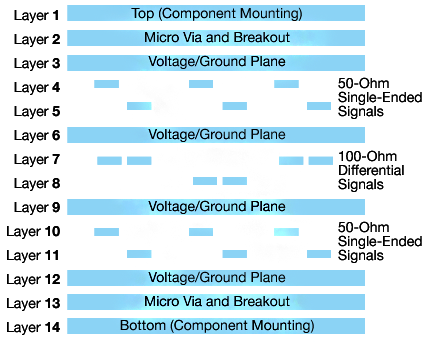
Achieving this requires discussion between the PCB layout engineer and the PCB supplier to determine the stack up of the board. The stack up and corresponding trace widths and separations are critical to implementing a controlled impedance board. Within most high-performance systems, both microstrip and stripline must be calculated correctly to provide a controlled impedance of 50 Ohms for single-ended signals and 100 Ohms for differential signals. This enables the hardware engineer to correctly terminate any transmission lines which occur using either on-chip or discrete termination.
It is also important within the stack up to ensure the voltage planes and the return planes are closely coupled to each other. This allows capacitive coupling. The substrate of the PCB between the planes can act like a decoupling capacitor, adding to the decoupling performance.
Figure 5: Example of a PCB Stack Up for Controlled Impedance Board
The design engineer must specify a series of constraints to the layout engineer at this stage as well. These will guide the placement of components, such as separating analog away from digital. They should also specify constraints on the grouping and length-matching of buses and signals within the design. To aid with this objective, the engineer might also specify a time of flight for the signal.
Cross talk between signals within the PCB should also be considered. Ensuring that signal traces are separated correctly reduces cross talk by reducing long parallel runs of signals on the same layer, or on layers above or below within a stripline structure. It is a good idea, if possible, to declare impedance-controlled layers between planes as vertical or horizontal routing, to ensure that tracks on different tracks do not have long parallel runs. Increasing the space between two traces on a PCB will reduce the cross talk. A good rule of thumb is to keep traces separated by at least three track widths. However, for more critical signals, this should be increased to five or even seven track widths.
Analog and digital signals should be kept as far apart as possible, and, whenever possible, separate analog returns and power supplies should be used. Neither digital nor analog signals should be routed referencing the other's plane, as it complicates the return current path and will degrade the system's performance.
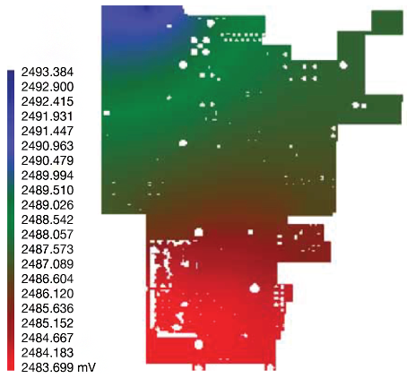
One of the most important stages towards the end of the layout, once the planes have been entered, is the validation of both the signal integrity of the completed design and power integrity. This validation may be an iterative process, more so for the power integrity, as the high currents required by the Processor, DSP, SoC, or FPGA core may lead to the need to adjust more planes to achieve the required voltage performance of the planes.
Figure 6: Example of a DC Power Analysis Result for a High-Power FPGA Application
Once the layout data pack has been released, we are able to then start manufacturing, commissioning, and testing the boards. But commissioning and testing is itself another Essentials course.
*Trademark. Xilinx is a trademark of Xilinx Inc. Other logos, product and/or company names may be trademarks of their respective owners.
Test Your KnowledgeBack to Top
Are you ready to demonstrate your Printed Circuit Board Design knowledge? Then take this 15-question quiz to see how much you've learned.
To earn the Printed Circuit Board Design badge, read through the learning module, attain 100% on the Quiz, leave us some feedback in the comments section, and give the learning module a star rating.


